PCB Fabrication Services

High-Quality PCB & FPC Manufacturing Solutions for Global Businesses
✔️ High-Precision Boards | ✔️ Fast Turnaround | ✔️ Competitive Pricing

Why Choose PCBArise for PCB Fabrication Services

PCBArise provides PCB fabrication services for prototypes, small batches, and volume production. We support multilayer PCBs, HDI PCBs, flexible PCBs, rigid-flex PCBs, high-frequency PCBs, heavy copper PCBs, controlled impedance, and advanced surface finishes for global electronics companies.

We support quick-turn prototypes, small batches, and volume production for industrial, automotive, medical, IoT, communication, and power electronics applications.

Our PCB Fabrication Services

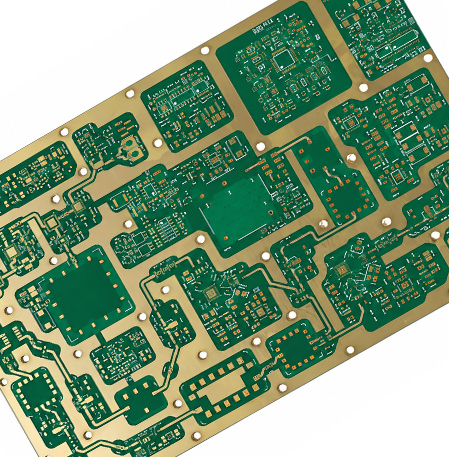
Advanced PCB Capabilities

● 1-layer to 60+ layer PCB fabrication

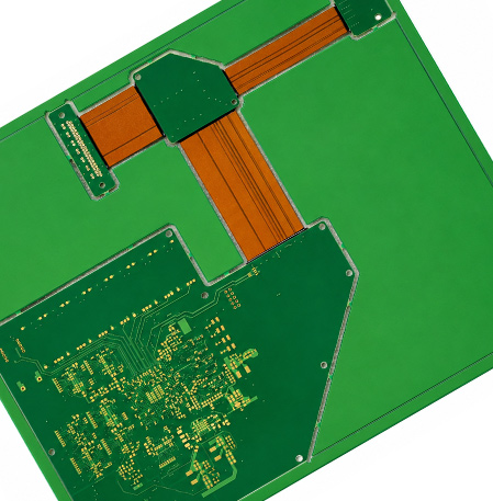
● HDI, rigid, flex, and rigid-flex PCBs

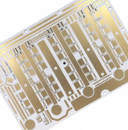
● High-frequency, heavy copper, and metal-core PCBs

● Blind/buried vias, microvias, and controlled impedance

Material Expertise

● FR-4 and high-Tg FR-4

● Rogers, Taconic, and other RF materials

● Aluminum, heavy copper, polyimide, ceramic, and specialty substrates

DFM Review Before Production

● Gerber, stack-up, and impedance review

● Drill, spacing, annular ring, and copper balance checks

● Manufacturability feedback before fabrication

Strict Quality Assurance

● AOI inspection and 100% electrical testing

● Impedance testing and microsection analysis when required

● IPC-A-600 Class 2/3 standards available

Fast Turnaround & Scalable Capacity

● Quick-turn prototypes

● Small-batch and pilot-run production

● Stable volume manufacturing

● Global delivery support

PCB Fabrication Process: From Gerber to Shipment

Understanding the PCB manufacturing process is crucial for ensuring quality and reliability in your electronic projects. Below is a comprehensive, step-by-step guide to how your design transforms into a physical board.

PCB fabrication process from Gerber file review to final shipment

Multilayer, HDI, Flexible and Rigid-Flex PCB Solutions

We specialize in a wide range of printed circuit board technologies to meet your specific engineering needs.

Rigid PCB and multilayer circuit board fabrication for electronic applications

Durable multilayer boards suitable for industrial, automotive, and consumer electronics. We provide high-precision fabrication ranging from standard FR-4 boards to complex multi-layer designs (up to 60+ layers). Our facilities are optimized for both quick-turn prototypes and high-volume production runs.

HDI PCB fabrication with microvias and high-density interconnect design

Featuring microvias, blind/buried vias, and fine lines for high-speed signal transmission. Essential for modern compact electronics.

Flexible PCB and FPC manufacturing for compact electronic devices

Flexible circuits designed for compact devices, wearables, and dynamic flex applications. Our FPC solutions utilize high-quality Polyimide (PI) to ensure durability in tight spaces without sacrificing signal performance. Ideal for smartphones, tablets, and medical devices.

Rigid-flex PCB manufacturing for complex three-dimensional electronic assemblies

The best of both worlds: combining the durability of rigid boards with the adaptability of flexible circuits. Perfect for complex 3D packaging requirements, reducing the need for connectors and improving reliability in aerospace and military applications.

High-frequency PCB fabrication for RF and microwave electronic applications

High-Frequency: Low-loss materials (Rogers, Taconic, Teflon) designed for RF and microwave applications where signal integrity is critical.

Metal core PCB and aluminum PCB manufacturing for thermal management

Superior thermal management solutions using Aluminum or Copper bases. Our MCPCBs are designed to dissipate heat efficiently, making them ideal for LED lighting, power supplies, and automotive electronics.

PCB Fabrication Capabilities Overview

我们的标准能力涵盖了大多数工业和商业电子需求。.

特点规格
层数1 - 40 层
基础材料FR-4(标准/TG170)、罗杰斯、聚酰亚胺(PI)、Taconic、铝、聚四氟乙烯、陶瓷
板厚0.1 毫米 - 10.0 毫米(标准:1.6 毫米)
最小轨迹宽度/间距2.5mil / 2.5mil(0.0625 毫米 / 0.0625 毫米)
Min Hole Size/strong>0.15毫米(机械钻孔),0.1毫米(激光钻孔)
最大长宽比12:1(通孔)
表面处理OSP、ENIG、含铅 HASL、无铅 HASL、浸锡/银、ENEPIG、金手指、镀金、硬金
铜厚度0.5 盎司 - 12 盎司(可提供重铜)
最小 BGA 焊盘直径8 mil
阻焊层颜色绿色(标准)、黑色、蓝色、红色、白色、黄色、紫色
丝印颜色白、黑、黄
阻抗控制±5% 公差

Multilayer PCB and HDI PCB Fabrication Capabilities

对于需要尖端技术和更严格公差的项目,我们的先进生产线能够满足要求。.

特点 规格
层数 多达 60 多层
电路板厚度公差 ±0.05毫米
最小轨迹宽度/间距 2mil / 2mil(0.05 毫米)
最小孔径 0.1毫米(机械钻孔),0.075毫米(激光钻孔)
最大长宽比 15:1(通孔)
表面处理 ENIG(金厚度 1u”-3u”)、ENEPIG、硬金(最大 50u”)、银、OSP
阻抗控制 ±3% 公差(严格)
人类发展倡议技术 任意层 HDI、堆叠和交错通孔、焊盘内通孔
人类发展倡议建设 1+N+1 至 4+N+4,任意层互连
导热性 铝质印刷电路板最高 3.0 W/m.k

Flexible PCB and Rigid-Flex PCB Fabrication Capabilities

我们的 FPC 专业技术包括高达 200,000 次的动态弯曲,以及屏蔽层、加强筋、ZIF 连接器和表面贴装元件的定制。.

特点规格
电路类型单面、双面、多层、刚柔结合
层数1 - 12 层
材料选择灵活:聚酰亚胺(Kapton)、PET、LCP
刚性: 高 Tg FR-4(用于刚性部分)
可应要求提供高级材料
板厚灵活区域: 0.1 毫米 - 0.6 毫米
整体 / 刚柔结合: 最大 3.2 毫米
铜重1/3 盎司至 2 盎司(12 微米至 70 微米)
最小轨迹/间距标准: 3/3 密耳(0.076 毫米)
高级 低至 2/2 密耳(0.051 毫米)
最小孔径激光钻孔: 0.1 毫米
机械钻孔: 0.15 毫米 - 0.2 毫米
表面处理选项ENIG(FPC 标准)、浸锡、浸银、OSP、选择性硬金
覆盖层选项聚酰亚胺 + 环氧树脂(黄/黑/白),照片成像覆盖层,柔性焊接掩模
加强筋选项FR-4、聚酰亚胺 (PI)、不锈钢、铝
弯曲半径静态: 3-6 倍厚度
充满活力 10-20 倍厚度
动态灵活能力设计经过优化,可在受控弯曲区域内实现 >100 万次弯曲循环
测试100% 电气测试、AOI 检测、动态挠性测试、可定制测试

按产品复杂程度和数量分列的交付周期

从快速原型设计到批量生产,我们都能提供灵活的时间安排,满足您的项目期限要求。.

标准交货时间(工作日):

产品类型原型(1-10 平方米)小批量(10-50 平方米)批量生产(>50 平方米)
双面(2 升)24-48 小时3-5 天7-9 天
多层(4-6 升)48-72 小时4-6 天8-10 天
多层(8-12 升)4-6 天7-10 天10-15 天
多层(12-18 升)6-8 天10-12 天12-18 天
多层(18 升以上)7-12 天12-15 天15-20 天
高密度(HDI)7-12 天12-15 天15-20 天
柔性印刷电路板(FPC)4-5 天6-8 天10-14 天
刚性-柔性7-10 天10-14 天15-20 天

请注意: 具体的交货时间将根据生产数据进行评估。. 可为样机提供加急服务(紧急订单)。请联系我们的销售团队了解具体要求。.

Get a PCB Fabrication Quote

上传您的 Gerber 文件,并在 24 小时内获得快速、专业的 PCB 报价。我们的工程团队将审查您的设计,确认关键规格,并帮助您顺利完成从原型到生产的整个过程。.

快速报价响应

免费 DFM 审查

原型和批量生产支持

原型无起订量

提供保密协议

点击或拖动文件至此处 Max 50MB - jpg、png、pdf、doc、xls、zip、rar、txt、csv
请留言
电话 +86 19129400135
电子邮件 [email protected]
WhatsApp 8619129400135
微信 19129400135
返回顶部

微信

微信二维码

所有产品

联系我们

请留言