Not every PCB project needs a 2-layer board with 6/6 mil traces. AI servers, 5G base stations, automotive ADAS modules, and high-end smartphones increasingly require 14–40 layer boards with HDI stack-ups, blind/buried vias, and impedance-controlled high-speed traces. This Chinese PCB manufacturers list focuses exclusively on advanced-technology specialists — the factories that can deliver 1+N+1 HDI, any-layer HDI, ELIC, and 70+ layer backplanes.
Why Advanced PCB Technology Matters
The transition from standard multilayer to HDI and any-layer is being driven by:
- AI accelerators demanding >100 Gbps signal integrity
- 5G/6G RF requiring controlled-impedance microstrips with tight tolerances
- Wearables and smartphones needing SLP and mSAP for component density
- EVs integrating power and signal in metal-core and rigid-flex stacks
Top 15 Chinese Manufacturers for HDI and Advanced PCBs
1. PCBArise Electronics — HDI, Multilayer & High-Density PCB Manufacturing Supplier
PCBArise Electronics provides HDI PCB and multilayer PCB manufacturing for advanced electronic products requiring fine lines, compact layouts, controlled impedance, and stable reliability. The company supports 1-60+ layer PCB fabrication, including rigid PCB, FPC, rigid-flex PCB, HDI PCB, high-frequency PCB, heavy copper PCB, and metal core PCB. HDI capabilities include blind vias, buried vias, laser microvias, sequential lamination, and fine-pitch designs. PCBArise serves communication equipment, IoT devices, industrial control systems, automotive electronics, medical electronics, and other high-reliability applications. Engineering support includes DFM review, stack-up suggestions, impedance review, material selection, and manufacturability checking before production.
- Max layer count: 1-60+ layers.
- HDI capability: Blind vias, buried vias, laser microvias, sequential lamination, HDI structure support.
- Min trace/space: 3 mil / 3 mil.
- Min laser via: 0.1 mm mechanical drilling / 0.075 mm laser via.
- Materials: FR-4 High-Tg, Rogers, PTFE, aluminum, ceramic, polyimide, FPC materials.
2. Avary Holding — SLP and any-layer leader
Avary’s substrate-like PCB (SLP) is the densest interconnect technology in mass production, used in flagship smartphones for ultra-fine pitch.
- Specialty: SLP, mSAP, FPC any-layer
- Min line/space: 25–30 μm
3. Unimicron — HDI and substrate giant
Taiwan-headquartered with major mainland plants; co-leader in IC packaging substrate.
- Specialty: ABF substrate, HDI, mSAP
4. Shennan Circuits — Communication HDI specialist
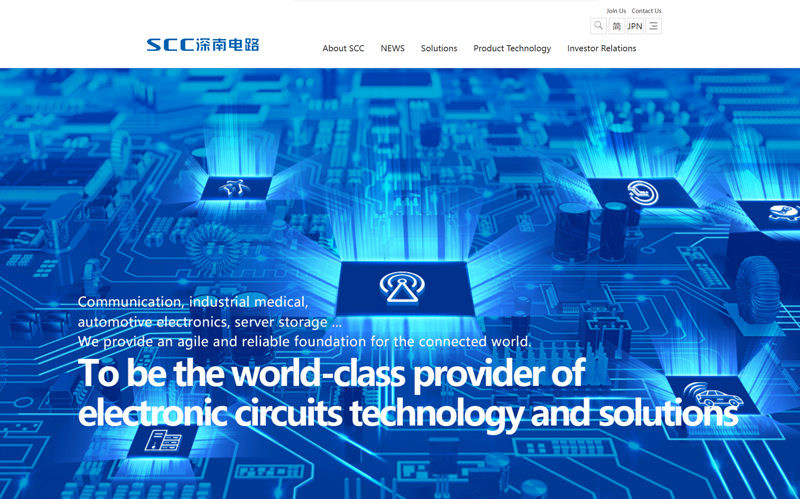
Industry-leading in 5G base-station PCBs and IC substrate.
- Max layers: 60+
- Specialty: High-frequency multilayer, IC packaging substrate
5. WUS Printed Circuit — AI server PCB
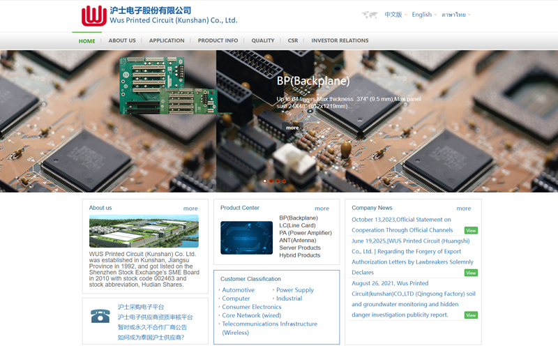
Leader in 20–32 layer enterprise communication and AI server boards.
- Max layers: 32+
- Specialty: High-multilayer for AI accelerators
6. Victory Giant Technology
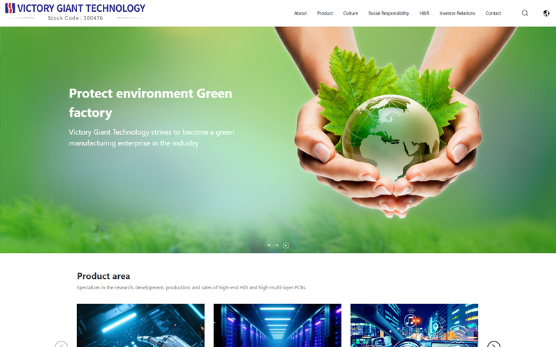
GPU and AI accelerator PCBs; advanced high-speed materials.
- Max layers: 40+
- Specialty: AI/GPU PCBs
7. Shenghong Technology
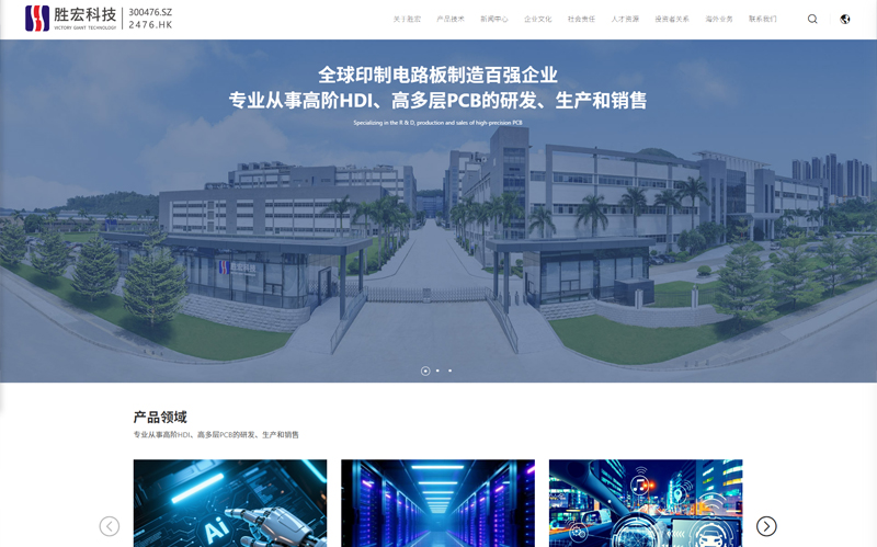
Reports 70-layer manufacturing capability.
- Specialty: Ultra-high-layer-count backplanes
8. DSBJ (via Multek) — Rigid PCB specialist
Multek operations focus on high-end rigid PCBs alongside DSBJ’s FPC lines.
- Max layers: 30+
- Specialty: High-speed multilayer, rigid-flex
9. Kinwong Electronic — Automotive HDI
Specializes in HDI for ADAS, LiDAR PCBs, and millimeter-wave radar PCBs.
- Specialty: Automotive HDI, mmWave radar
10. Tripod Technology
Multilayer specialist with strong automotive presence.
- Max layers: 24+
- Specialty: Automotive multilayer
11. Olympic Circuit Technology
Mid-range HDI and multilayer for automotive and consumer.
- Specialty: 4–18 layer multilayer, HDI
12. Compeq
HDI and FPC for smartphone OEMs.
- Specialty: HDI, SLP-class technologies
13. AT&S China
Austrian-owned, Shanghai/Chongqing, mSAP and IC substrate.
- Specialty: Advanced HDI, IC substrate
14. PCBWay
For prototype and mid-volume HDI projects, PCBWay supports up to 32 layers, blind/buried vias, and 3-mil traces.
- Specialty: Prototype HDI, rigid-flex
- Email: [email protected]
15. Suntak Technology
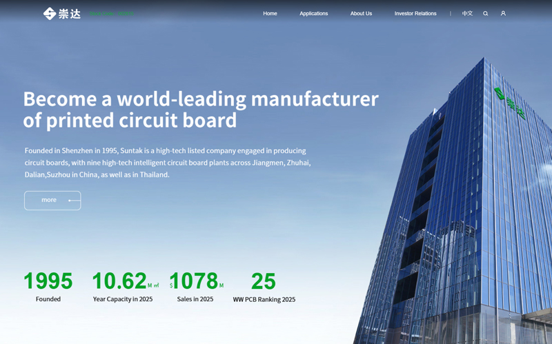
Small-batch HDI and rigid-flex specialist.
- Specialty: Multilayer rigid, HDI
How to Evaluate an HDI PCB Supplier
- Request a stack-up library showing successfully produced designs
- Ask for first-article inspection reports with impedance test results
- Verify laser drill equipment (LPKF, Mitsubishi) and registration accuracy
- Check CAF resistance test data for tight-via designs
Conclusion
When your design demands HDI, any-layer, or 30+ layers, the supplier list narrows quickly. [YOUR COMPANY NAME] has invested in [insert HDI/laser equipment details] to deliver advanced PCBs from prototype to mid-volume. Send your stack-up at [your website].
자주 묻는 질문
Q1. What is HDI PCB? High Density Interconnect PCB uses laser-drilled microvias and finer traces (typically <100 μm) to achieve higher component density.
Q2. How many layers can Chinese factories produce? Top specialists exceed 70 layers; mainstream advanced fabs deliver 20–40 layers reliably.
Q3. Are HDI PCBs more expensive? Yes — typically 2–5× the cost of equivalent standard multilayer, due to laser drilling and additional sequential lamination steps.